| ARP Axxe /\ | ||
|
Check out my YouTube channel. |
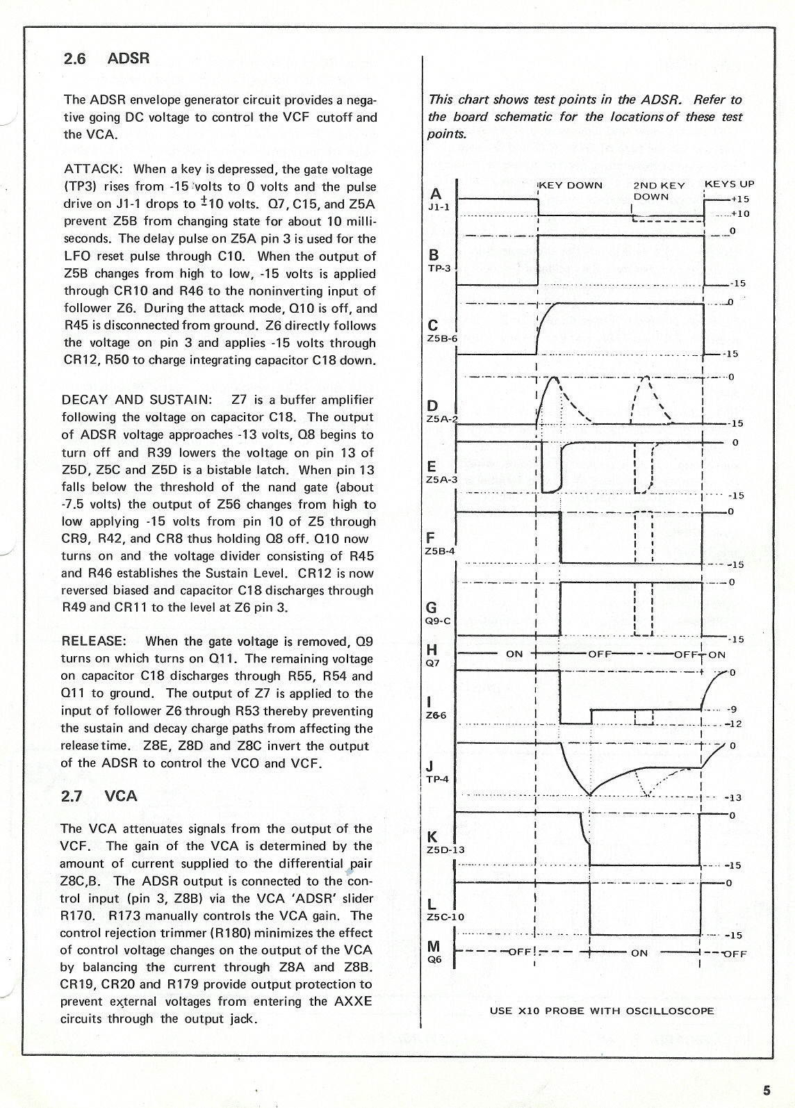
The circuits of the Axxe are designed so that there is a 10ms delay between when the incoming gate voltage goes high and when the ADSR actually starts its attack. Here is a page from the Axxe service manual with a description.
During this 10ms time period, the LFO gets reset. Why did they design it this way? I have no idea. This annoying circuit does not seem to be present on the Odyssey.
The delay before the attack first became annoying to me when I was driving the Axxe from the GR-300 Envelope-to-Gate converter. My converter circuit is fast, and the delay of the Axxe was noticeable when trying to pick very quickly. Now I am running into the same annoyance when driving the Axxe from the Continuum Voltage Converter, which is also blindingly fast.
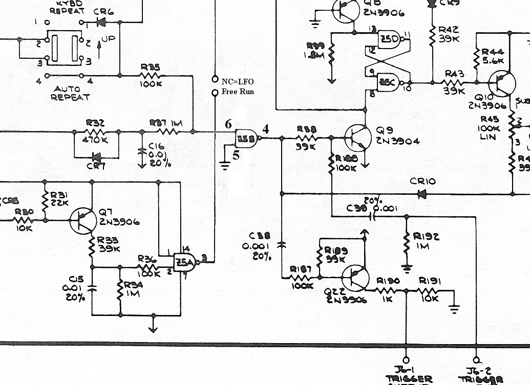
So I came up with a modification to get rid of the delay. Here is a schematic of the original circuit, which I've cleaned up a bit to make it more readable:

The NAND gate Z5B prevents the Gate signal (coming into pin 6) from getting through to its output until after the 10ms pulse from Z5A pin 3 (coming into pin 5) has gone from -15V back up to 0V. My mod is simply to disconnect pin 5 from the pulse and tie it to ground, so the NAND gate will always pass the signal through without waiting for the 10ms pulse to be over.
On the Axxe, the LFO always resets every time there is a gate signal. I didn't like this either, so I cut another trace to allow the LFO to "Free Run". If you wanted to, you could add a switch between the two halves of the cut trace (shown in the schematic below as two terminals) to allow switching "Free Run" on and off.
Here is the schematic of the circuit with both mods performed:
On the circuit board, the "Fast Axxe" mod involves cutting the trace between Z5-3 and Z5-5 (shown as a red line below) and adding a jumper wire between Z5-5 and Z5-1, which is ground (shown in blue).
The "LFO Free Run" mod invloves cutting the trace going out from pin 3 (shown as a green line). If you want to add an "LFO Free Run" switch, then hook the switch to the two halves of the trace after you have made the cut shown in green.
Here is a diagram showing both mods.
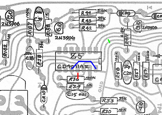
The above diagram shows the circuit board as if you are looking at it from the solder side. The components are drawn as they would look if you could see through the board.